D Flip Flop Truth Table
It is the drawback of the SR flip flop. Use the following state encoding.

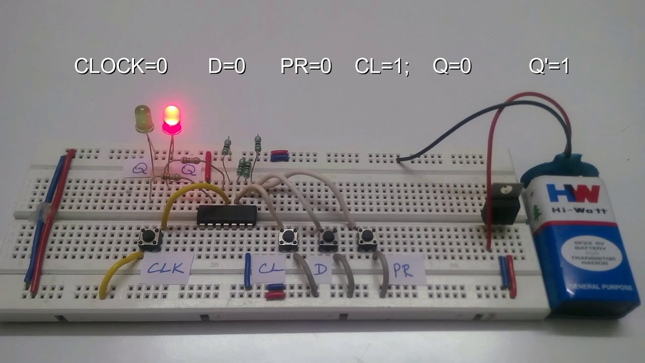
Ece 2610 D Flip Flip With Sr Flip Flip Included Diagram Logic Symbols
Both the inputs of the JK Flip Flop are connected as a single input T.

. Analysing the above assembly as a three stage structure considering previous stateQ to be 0. Override the feedback latching action. The D flip-flop can be viewed as a memory cell a zero-order hold or a delay line.
Qold is the output of the D flip-flop before the positive clock edge. D-latch is a level Triggering device while D Flip Flop is an Edge triggering device. In SR NAND Gate Bistable circuit the undefined input condition of SET 0 and RESET 0 is forbidden.
Will Labours GST U-turn do the Government much damage. It is a clocked flip flop. Here as soon as clear input is activated.
Preset and Clear both are different inputs to the Flip Flop. The following is the state transition table for a Moore state machine with one input one output and four states. At other times the output Q does not change.
In other word it retains its value. Make the flip flop in set stateQ1 the trigger passes the S input in the flip flop. For asynchronous clear the clear signal is independent of the clock.
Qp1 simply suggests the future values to be obtained by the JK flip flop after the value of Qp. Dual-edge triggered flip-flop. The name T flip-flop is termed from the nature of toggling operation.
The D flip-flop captures the value of the D-input at a definite portion of the clock cycle such as the rising edge of the clock. T Flip Flop. Draw K-Maps using required flipflop inputs and obtain excitation functions for.
Below is the logical circuit of the T Flip Flop which is formed from the JK Flip Flop. While this implementation of the J-K flip-flop with four NAND gates works in principle there are problems that arise with the timing. When the enabler input E is set to 1 the output Q can be set to the Data input D.
Digital flip-flops are memory devices used for storing binary data in sequential logic circuitsLatches are level sensitive and Flip-flops are edge sensitive. Each operator maintains its own boolean state even across calls to a subroutine that contains it. In these cases by creating D flip-flop we can omit the conditions where S R 0 and S R 1.
Whats more the details of the ill-fated tax proposal are almost too technocratic to even comprehend or care about. Edge Triggered D flip flop with Preset and Clear. Thus comparing the NAND gate truth table and applying the inputs as given in D flip-flop truth table the output can be analysed.
The table is then completed by writing the values of S and R required to get each Qp1 from the corresponding Qp. The waveforms pertaining to the same are presented in Figure 3. JK Flip Flop Construction Logic Circuit Diagram Logic Symbol Truth Table Characteristic Equation Excitation Table are discussed.
Both can be synchronous or asynchronousSynchronous Preset or Clear means that the change caused by this single to the. In this article we will discuss about SR Flip Flop. Thats why delay and.
Write the corresponding outputs of sub-flipflop to be used from the excitation table. The truth table for a JK Flip Flop has been summarised in Table I below. It stands for Set Reset flip flop.
D flip flop is actually a slight modification of the above explained clocked SR flip-flop. In D flip-flop if D 1 then S 1 and R 0 hence the latch is set on the other hand if D 0 then S 0 and R 1 hence the latch is reset. It is mainly caused by an asynchronous setpreset or clearreset signal.
Characteristics and applications of D latch and D Flip Flop. D Flip-flop Data JK Flip-flop Jack-Kilby T Flip-flop Toggle Out of the above types only JK and D flip-flops are available in the integrated IC form and also used widely in most of the applications. A simple truth table will help us describe the design.
Implement a JK flip-flop with only a D-type flip-flop and gates. The operator is bistable like a flip-flop and emulates the line-range comma operator of sed awk and various editors. It remains as its previous value.
When D flip-flop generates output independent of the clock signal then the output produced may be asynchronous. The disadvantage of the D FF is its circuit size which is about twice as large as that of a D latch. This is known as a Gated D Latch.
When D 1 and CLOCK HIGH. That captured value becomes the Q output. Moreover it is to be noted that the working of the negative edge-triggered flip-flop is similar to that of positive-edge triggered one except that the changes occur at the trailing edge of the clock pulse instead of its leading edge.
A JK flip-flop has the below truth table. SR Flip Flop- SR flip flop is the simplest type of flip flops. The edge triggered flip Flop is also called dynamic triggering flip flop.
Returns a boolean value. D Flip Flop to JK Flip Flop. D flip-flop Truth table reset and clock input Asynchronous D flip flop.
Behavioral Modeling of D flip flop with Asynchronous Clear. Truth Table of T Flip Flop The upper NAND gate is enabled and the lower NAND gate is disabled when the output Q To is set to 0. The problem for.
Q N1 D. Power consumption in Flip flop is more as compared to D latch. Draw the truth table of the required flip-flop.
Probably not its insignificant in the greater scheme of things. Lose the control by the input which first goes to 1 and the other input remains 0 by which the resulting state of the latch is controlled. Construction of SR Flip Flop- There are following two methods for constructing a SR flip flop- By using NOR latch.
The timing pulse must be very short because a change in Q before the clock pulse goes off can drive the circuit into an oscillation called racingModern ICs are so fast that this simple version of the J-K flip-flop is not practical we put one together in. A2b00 B2b01 C2b10 D2b11. When the enabler input E is set to 0 the output Q cannot be changed.
The D input is passed on to the flip flop when the. From the figure you can see that the D input is connected to the S input and the complement of the D input is connected to the R input. The truth table of a D-Type Flip-Flop circuit is as follows.
The truth tables for the flip flop conversion are given below. There are many applications where separate S and R inputs not required. Most likely the flip-flop will soon be forgotten.
Edge Triggered D type flip flop can come with Preset and Clear. Create circuit from truth table. This type of modeling is simple since it does not involve using complex circuitry.
Force both outputs to be 1. Here in this article we will discuss about T Flip Flop. Characteristics Equation for D Flip Flop.
It means that the latchs output change with a change in input levels and the flip-flops output only change when there is an edge of controlling signalThat control signal is known as a clock signal Q. JK flip flop is a refined and improved version of the SR flip flop. The circuit diagram and truth table is given below.
Implement only the state transition logic and output logic the combinational logic portion for.

T Flip Flop Circuit Truth Table And Working Electronic Circuit Projects Electronics Circuit Circuit Projects
D Flip Flop Circuit Truth Table Working

Digital Flip Flops Sr D Jk And T Flip Flops Sequential Logic Circuits Nursing Student Tips Circuit Energy Technology
What Are Flip Flops In Electronics A Flip Flop Is An Electronic Circuit That Can Store Single Bit Binary Data Eith Circuit Digital Circuit Electronics Circuit
No comments for "D Flip Flop Truth Table"
Post a Comment